Philip D. Rack |
UT office (865)
974-5344 ORNL office (865) 241-1598 fax (865) 974-4115 |
Combinatorial Thin Film Synthesis for Rapid Materials Discovery
One of the cornerstone pieces of equipment in my laboratory is a multisource rf magnetron sputtering system capable of depositing thin film metals, semiconductors, and insulating materials. The system consists of a 20” diameter stainless steel chamber pumped with a 550lps turbomolecular pump. The system is equipped with a load-lock chamber that can currently accommodate up to 6” substrates and has a routine base pressure ~ 1x10⁻⁸ Torr. The sputtering system has 4-2” sources (scalable to 5) with in-situ source tilting capabilities which allows thin film materials (metals, semiconductors, and insulators) to be deposited in a combinatorial or layered fashion. The sources have a variable magnetron assembly for balanced, unbalanced and magnetic materials modes and are powered by 500 Watt rf power supplies and matching networks. Each source has a localized gas delivery for optimized deliver of the inert sputter gas. In addition, the substrate holder assembly has a localized gas injection for preferential delivery of reactive gases to the substrate for reactive sputtering. The compositions as a function of position can be uniform by rotating the substrate, or a deliberate composition gradient can be introduced by depositing onto a stationary substrate. By varying the individual source powers and tilt angles, large composition gradients can be realized across a single wafer leading to rapid materials discovery. To enhance/modify the thin film quality the substrate is equipped with a heater (up to 800oC) and bias sputtering capabilities. Figure 1 shows a schematic of the multi-source sputtering system and a digital photograph of the system while depositing a combinatorial ternary Fe-Cr-Ni thin film sample.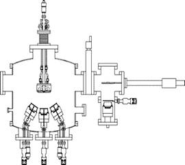
Figure 1. a) Schematic of the multi-source rf-magnetron sputtering system and
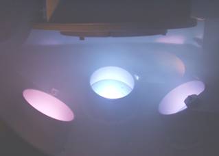
digital photograph of the sputtering system while depositing a combinatorial ternary phase diagram of Fe-Ni-Cr.
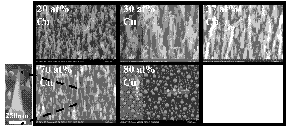 Figure 2.
Scanning electron micrographs along of cabon nanofibers with
varying copper concentration in the catalyst alloy prepared via the
combinatorial thin film sputtering technique.
Figure 2.
Scanning electron micrographs along of cabon nanofibers with
varying copper concentration in the catalyst alloy prepared via the
combinatorial thin film sputtering technique.
Experimental Phase Diagram Determination
Equilibrium and non-equilibrium phase diagram determination is
typically a very labor intensive process requiring the preparation
and characterization of numerous alloy samples.
To rapidly identify the equilibrium and non-equilibrium phase
diagram of Cr-Ni-Fe, ternary libraries were prepared by
co-sputtering Cr, Fe, and Ni on a single-crystal sapphire
substrates. Subsequent
to the depositing five samples, four of the samples were annealed at
200, 400, 600, and 800C.
Structural and compositional maps of the alloys were produced
using synchrotron radiation and simultaneous detection of 2D
diffraction patterns and x‑ray fluorescence spectra.
Figure 3 shows the phase diagram evolution for this ternary
alloy as a function of annealing temperature.
Good agreement between the measured and calculated phase
diagram is demonstrated which illustrates the utility of this
approach for materials development.
As-deposited a very non-equilibrium structure exists with a
metastable
a-manganese
simple cubic structure (shaded area).
When the alloy is annealed the grain size increases (as
determined with the Scherrer formula) and the phases evolve into the
thermodynamically stable phase.
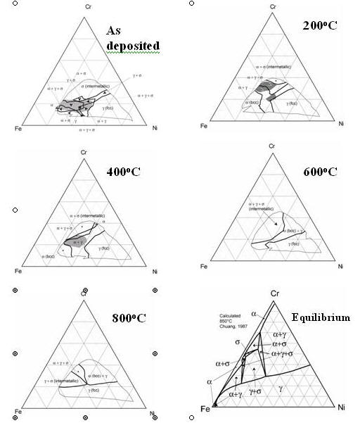 Figure 3.
Phase diagram evolution for Fe-Ni-Cr ternary alloy.
Figure 3.
Phase diagram evolution for Fe-Ni-Cr ternary alloy.
References
-
J.D. Fowlkes, P.D. Rack, J.M. Fitz-Gerald, “Ultraviolet emitting (Y1-xGdx)2O3-z thin films deposited by rf magnetron sputtering: structure – property – thin film processing relationships” Thin Solid Films, (in press).
-
J.D. Fowlkes, P.D. Rack, J.M. Fitz-Gerald, Ultraviolet emitting (Y1-xGdx)2O3-z thin films deposited by rf magnetron sputtering: Combinatorial modeling, synthesis, and rapid characterization, Thin Solid Films, Vol. 510, no. 1-2, pp. 68-76 (July 2006).
-
Yuepeng Deng, Jason D. Fowlkes, Philip D. Rack, James M. Fitz-Gerald, Thin Film rf Magnetron Sputtering of Gadolinium Doped Yttrium Aluminum Garnet Ultraviolet Emitting Materials, Journal of Optical Materials Vol. 29 pp.183-191 (November 2006).
-
Yuepeng Deng, Jason D. Fowlkes, James M. Fitz-Gerald, Philip D. Rack, Combinatorial Thin Film Synthesis of Gd-doped Y3Al5O12 Ultraviolet Emitting Materials, Applied Physics A. 80 no. 4, pp. 787-789 (February 2005).
-
Yuepeng Deng, Y. Guan, Philip D. Rack, Combinatorial Synthesis and Parameter Optimization of Chromium-doped Yttrium Aluminum Garnet Thin Film Sputtering, Thin Solid Films, vol 29, no 2-3, pp. 183-91 (Novemeber 2006).
-
Seung-Ik Jun, Anatoli V. Melechko, Timothy E. Mcknight, Michael L. Simpson, Philip D. Rack “Electrical and microstructural characterization of molybenum tungsten electrodes using a combinatorial thin film sputtering technique” Journal of Applied Physics Vol. 97 059046 pp. 1-6 (March 2005).
-
Yuepeng Deng, Yinfeng Guan, Jason D. Fowlkes, S.Q. Wen, George M. Pharr, Fengxiao Liu, Peter K. Liaw, C.T. Liu, Philip D. Rack, A combinatorial thin film sputtering approach for synthesizing and characterizing ternary ZrCuAl metallic glasses, Intermetallics (in press).
-
A. Rar, J. Frafjord, Jason D. Fowlkes, E. D. Specht, P. D. Rack, M. L. Santella, E.P. George, and G. M. Pharr, “PVD Synthesis and High-Throughput Property Characterization of Ni- Fe- Cr Alloy Libraries” Journal of Measurement Science & Technology, Vol 16, pp. 46-53 (January 2005).
-
E.D. Specht, P.D. Rack, A. Rar, G.M. Pharr, E.P. George, J.D. Fowlkes, H. Hong, and E. Karapetrova, “Metastable Phase Evolution and Grain Growth in Annealed Nanocrystalline Cr-Fe-Ni Films” Thin Solid Films (in press).
-
K. L. Klein, A. V. Melechko, P. D. Rack, J.D. Fowlkes, H. M. Meyer, and M. L. Simpson, “Cu-Ni composition gradient for the catalytic synthesis of vertically aligned carbon nanofibers” Carbon Vol. 43, Iss. 9, pp. 1857-1863 (August 2005).
Research directions
- Combinatorial thin film synthesis for rapid materials discovery
- Materials integration and nanofabrication for advanced device application
- Nanoscale focused electron beam stimulated processing. Below is a summary of these three research focus areas.