Philip D. Rack |
UT office (865)
974-5344 ORNL office (865) 241-1598 fax (865) 974-4115 |
Nanofabrication
My group has been and is involved in advanced nanofabrication of advanced biological, electronic, and optoelectronic devices. In particular we devise nanofabrication schemes for “non-traditional” device architectures that involve “non-traditional” materials integration. One current example is described below and the following link (pdf) is a compilation of several programs that my group has worked on.
Active Matrix Thin Film Transistor Intracellular Probe Array
An enormous body of knowledge has been accumulated about intracellular processes using the classical techniques of biochemistry, in which processes and structures are analyzed in subcellular fractions, which are produced after disrupting cells. The next biological frontier is in understanding how all these processes take place within the highly organized and ordered environment of the living cell. While advances in molecular biology and imaging technology are providing enormous insight into the genetic code and cellular structure, our ability to monitor detailed, ongoing processes inside the intact cell remains extremely limited. This limitation is largely technological – our current instruments are simply not on the same scale as the cell and its components. Recent critical developments at Oak Ridge National Laboratory (ORNL) in the fabrication of vertically aligned carbon nanofiber arrays now offer the opportunity to design nanoscale molecular probing devices that function at the scale necessary to map cellular processes at resolutions well below the diffractive limit of optical microscopy, and to interface these probes between single, living cells and the macroscopic world. Initial work at ORNL utilized single probe arrays (i.e. a single nanofiber per lead). Figure 1 illustrates a VACNF single probe device. Recently I have collaborated with the group at ORNL to integrate the VACNF intracellular probes with an active matrix thin film transistor array to increase the device density.
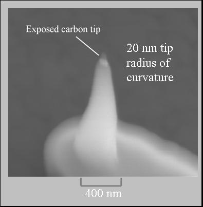
Figure 1. An individually addressable carbon nanofiber intracellular probe on an electrical interconnect.
Figure 4 illustrates the current process flow for the TFT array and an SEM cross-section of a completed device.
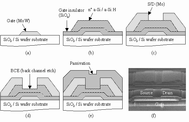
Figure 4.
Process sequence of TFT fabrication; (a) gate electrode, (b)
active (gate SiOx, a-Si:H, n+ a-Si), (c)
source-drain electrode, (d) back channel etching, (e) passivation,
(f) cross-sectional SEM image of TFT array.
Figure 5 illustrates the process flow for the current integration scheme with an SEM image demonstrating the growth of the nanofibers on the molybdenum drain electrodes.
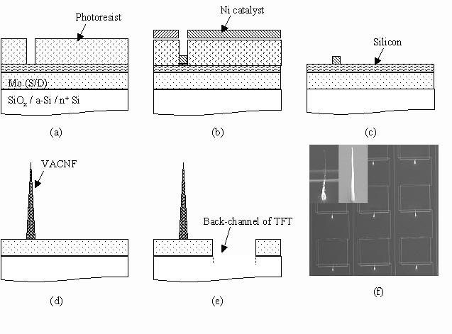
Figure 5. VACNF growth and source-drain patterning in TFT fabrication process; (a) photolithography, (b) Ni catalyst deposition by RF sputtering, (c) Ni lift-off by dipping into acetone for 1 hour, (d) growing VACNF in DC-PECVD, (e) source-drain electrode patterning and back-channel etching by photolithography and dry etching (RIE), (f) SEM image of VACNF just before source-drain patterning.
References
- Seung-Ik Jun, Anatoli V. Melechko, Timothy E. Mcknight, Michael L. Simpson, Philip D. Rack,Electrical and microstructural characterization of molybenum tungsten electrodes using a combinatorial thin film sputtering technique, Journal of Applied Physics Vol. 97 059046 pp. 1-6 (March 2005).
- Seung-Ik Jun, Anatoli V. Melechko, Timothy E. Mcknight, Michael L. Simpson, Philip D. Rack Characterization of reactively sputtered silicon dioxide thin films for fully sputtered metal-insulator-semiconductor switching devices, Electronics Letters, Vol 41, Iss. 14, No. 07, pp. 59 – 60 (July 2005)
- Seung-Ik Jun, Anatoli V. Melechko, Timothy E. Mcknight, Michael L. Simpson,
Philip D. Rack, DC substrate bias effects on amorphous silicon sputter
deposited films and integration and characterization of a sputter deposited thin
film transistor array, Applied Physics Letters Vol. 87, No. 13,
pp. 132108-1-3 (September 2005).
- Seung-Ik Jun, Anatoli V. Melechko, Timothy E. Mcknight, Michael L. Simpson, Philip D. Rack, Low Temperature Solid Phase Crystallization of Amorphous Si Thin Films Deposited with RF Magnetron Sputter Deposition with Substrate Bias, Applied Physics Letters Vol 89, no. 2, p 22104-1-3 (July 2006).
- Seung-Ik Jun, Anatoli V. Melechko, Timothy E. Mcknight, Michael L. Simpson,
Philip D. Rack, Electrical
characterization of amorphous silicon thin film transistors fabricated by rf
magnetron sputtering with substrate bias, Microelectronic Engineering
(submitted 6/06).
Research directions
- Combinatorial thin film synthesis for rapid materials discovery
- Materials integration and nanofabrication for advanced device application
- Nanoscale focused electron beam stimulated processing. Below is a summary of these three research focus areas.